Nano-system Fabrication Facility (NFF)
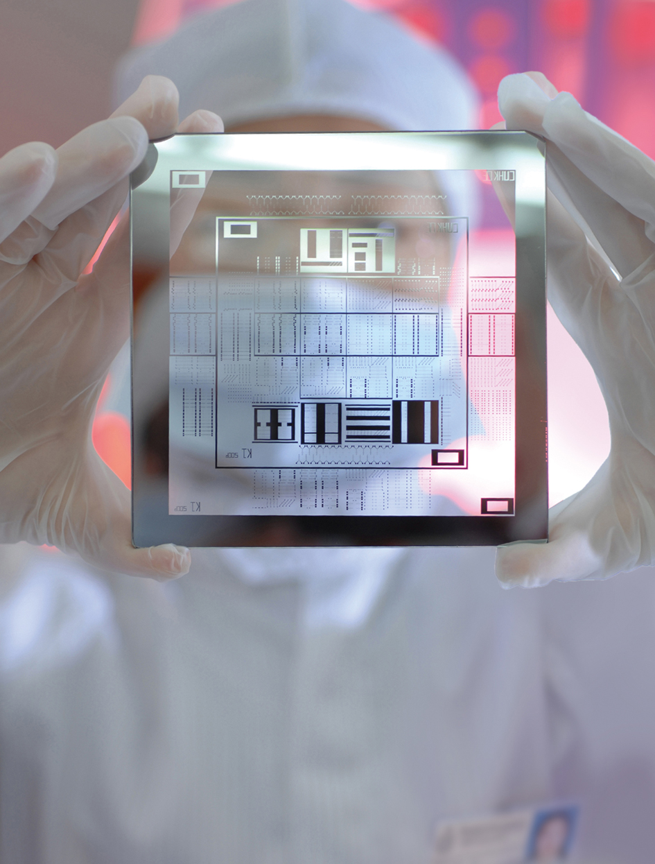
The Nano-system Fabrication Facility (NFF) of the Hong Kong University of Science and Technology (HKUST) is the first nanofabrication laboratory established at a tertiary institution in Hong Kong since 1991. Its mission is to provide fabrication facilities in support of research and teaching in micro/nano devices and systems. As a University's centralized research facility, NFF aims to support not only individual faculty members of HKUST but also researchers from local institutions in the area of micro/nano devices and systems. Mainland and overseas institutions as well as private sectors are also welcome to approach NFF for technical collaborations.
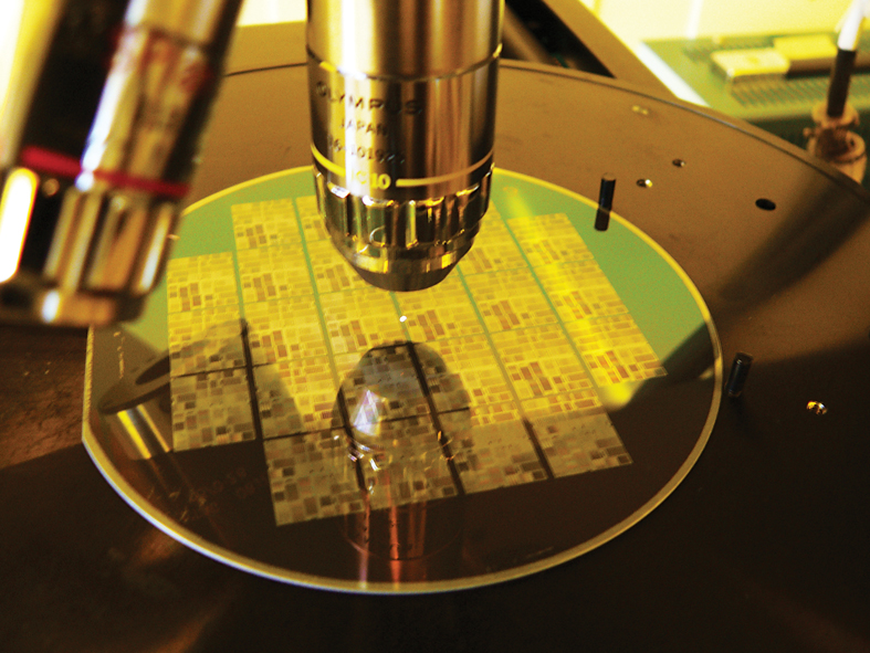
The NFF in HKUST boasts class 100 cleanroom, a state of the art Electron beam lithography system and a complete 4-inch silicon wafer processing line, offering photolithography, thermal diffusion and oxidation, thin-film deposition, dry/wet etching, metallization, implantation, and mask making services. The aim of NFF is to to explore and develop advanced nano-electronics technologies in the areas of:
- 3D Nano-electronics Devices
- Display Technology
- Micro-sensors
- Micro-Electro Mechanical System
- Silicon Photonics Technology
- Power Semiconductor Devices and Technology
- Advanced Packaging Program
- Advanced Process Module Development
- Gene Chip
- Compound Semiconductor Technology
Material Characterization and Preparation Facility (MCPF)
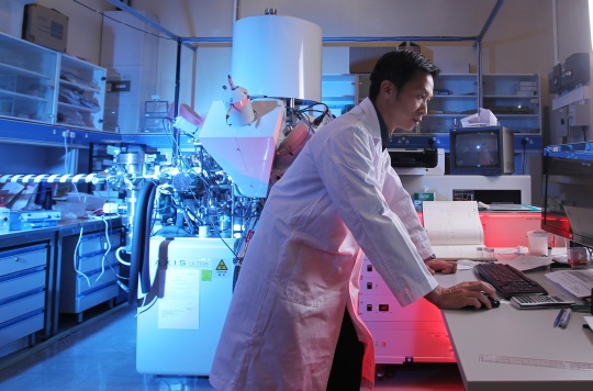
The Material Characterization and Preparation Facility (MCPF) of the HKUST provides preparation, characterization and analysis facilities for various advanced materials. The facility houses a wide variety of state of the art multi-disciplinary instrumentation with support of a dedicated and experience staff. MCPF mainly consists of eleven main research laboratories for sample preparation, optical characterization, surface analysis, electron microscopy, scanning probe microscopy, electrical and magnetic characterization, thin film deposition, thermal analysis, X-ray diffraction. Extensive training and regular workshops are also offered by the MCPF for both in-house and commercial clients.
Device Characterization Lab (DCL)
The Device Characterization Lab (DCL) is a multi-purpose laboratory for semiconductor-device characterization and integrated-circuit testing. The laboratory is equipped with a variety of advanced equipment for characterizing electronic devices, optoelectronic devices, power devices, and integrated circuits in both wafer and packaged forms. In addition, facilities for wafer dicing and packaging are also available. Specific equipment includes semiconductor parameter analyzers, capacitance meters, oscilloscopes, system controllers, IC testers, and an infrared video inspection system. A number of systems are equipped for automatic software-driven measurements